Theme: Design
the data path of an 8051 CPU ¾ on
the basis of the RAM and ALU practice
result of last week
Task
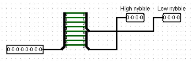
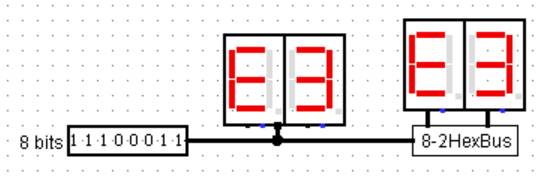
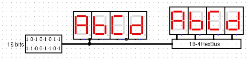
1: Use hexadecimal displays to show the
hexadecimal value on the bus
|
Circuit |
Appearance |
Connected |
|
|
8-2HexBus
|
|
|
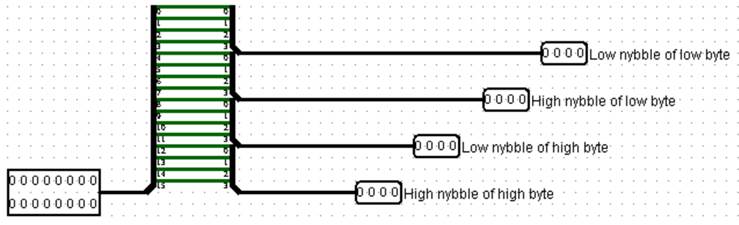
8-2HexBus_2
|
||
|
|
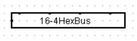
16-2HexBus
|
|
|
16-2HexBus_2
|
Task
2: Design around the ALU and Acc
|
What to consider? |
What are the Ain and Bin of the ALU? |
|
|
What instructions need to use the ALU? |
|
|
|
When to update Acc with ALU result? |
|
|
|
|
|
Instruction summary (See http://www.keil.com/dd/docs/datashts/atmel/at_c51ism.pdf)
|
Instruction |
Operand 1 |
Operand 2 |
|
|
ADD, ADDC, SUBB |
A |
Rn Direct @Ri #imm |
|
|
ANL, ORL, XRL |
A |
Rn Direct @Ri #imm |
|
|
direct |
A #imm |
|
|
|
|
|
|
|
|
|
|
|
|
Note: Rn, @Ri, & direct data are located in the RAM.
|
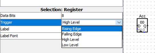
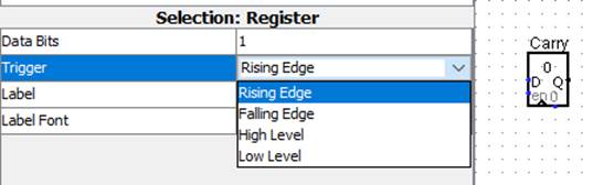
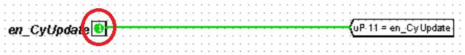
Register for Acc: Choose the trigger type. |
Carry flag: Choose the trigger type.
|
Task
3: Design around the 256-byte RAM
|
What to consider? |
What data to write (store)? |
Acc, Rn, direct, @Ri |
|
What data to read (load)? |
Rn, direct, @Ri |
|
|
What destination to read (load) to? |
Acc (through Ain or Bin), direct, @Ri |
|
|
|
|
|
|
|
|
Task 4: Finish the circuit design
Task
5: Run the test program
|
Circuit |
Test Program |
|
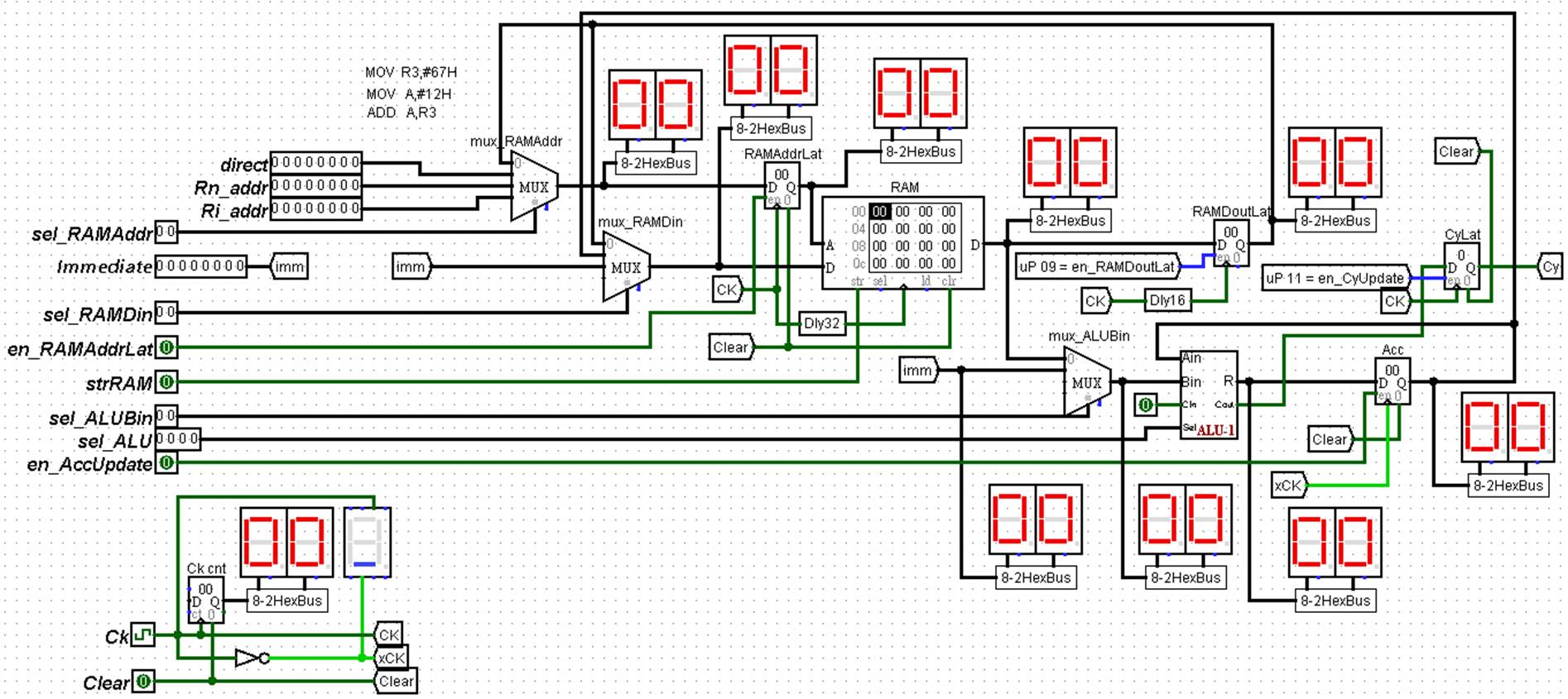
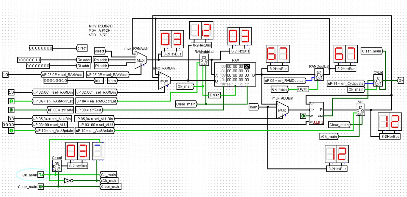
dataPath-2021Fall.circ |
MOV R3,#67H
MOV A,#12H ADD
A,R3 |
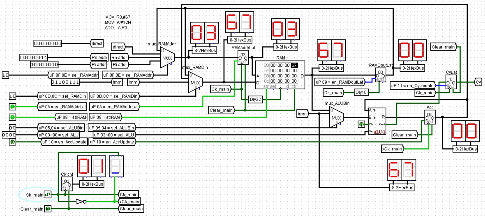
Before
running MOV R3,#67H
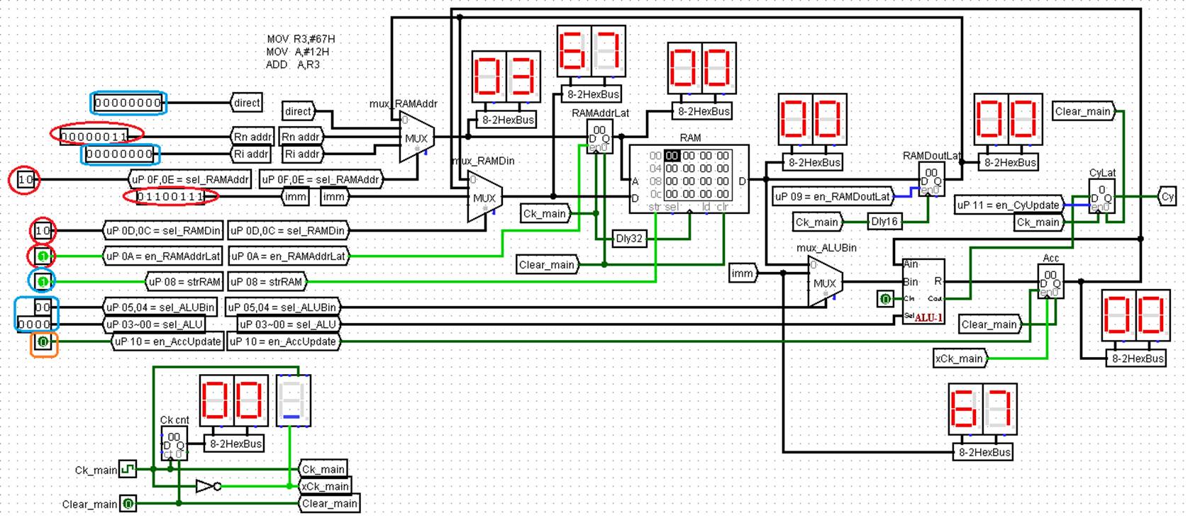
![]()
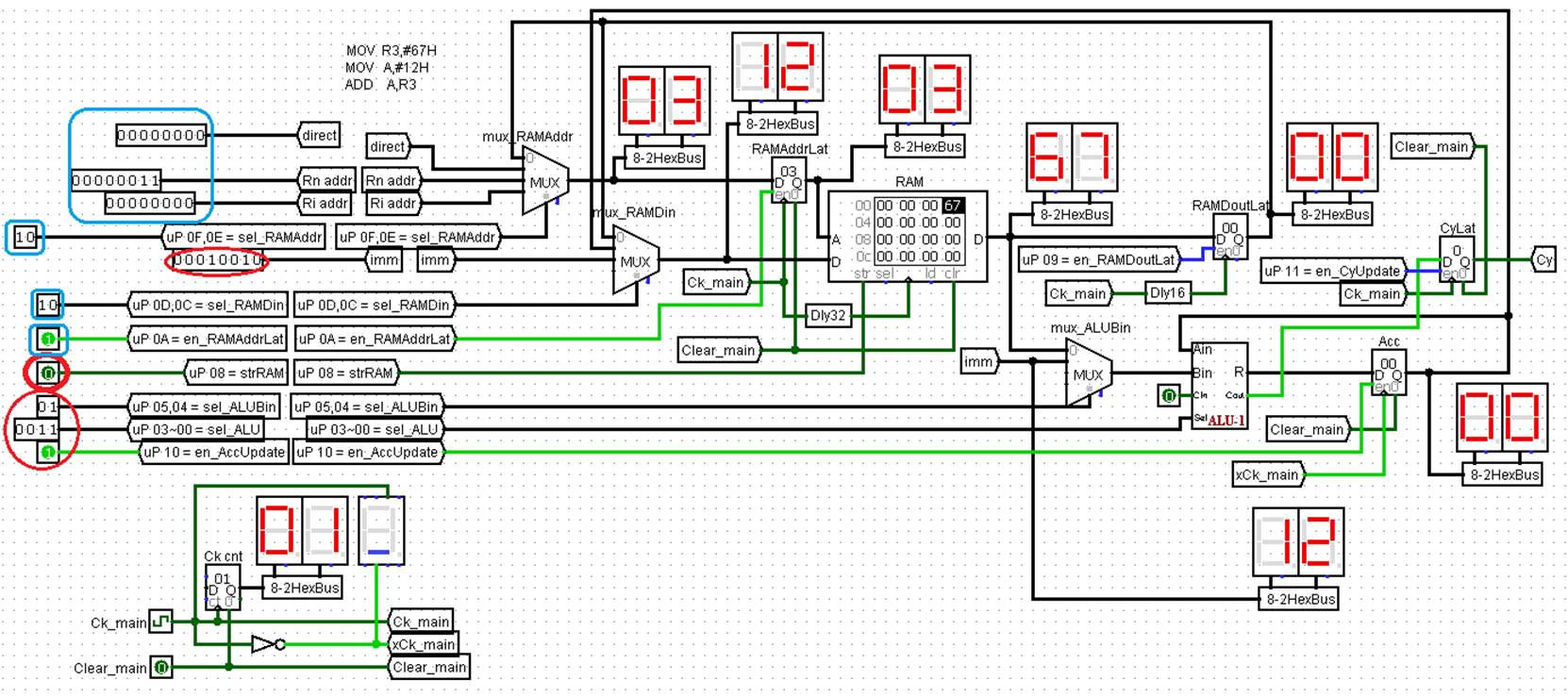
After positive edge of CK
![]()
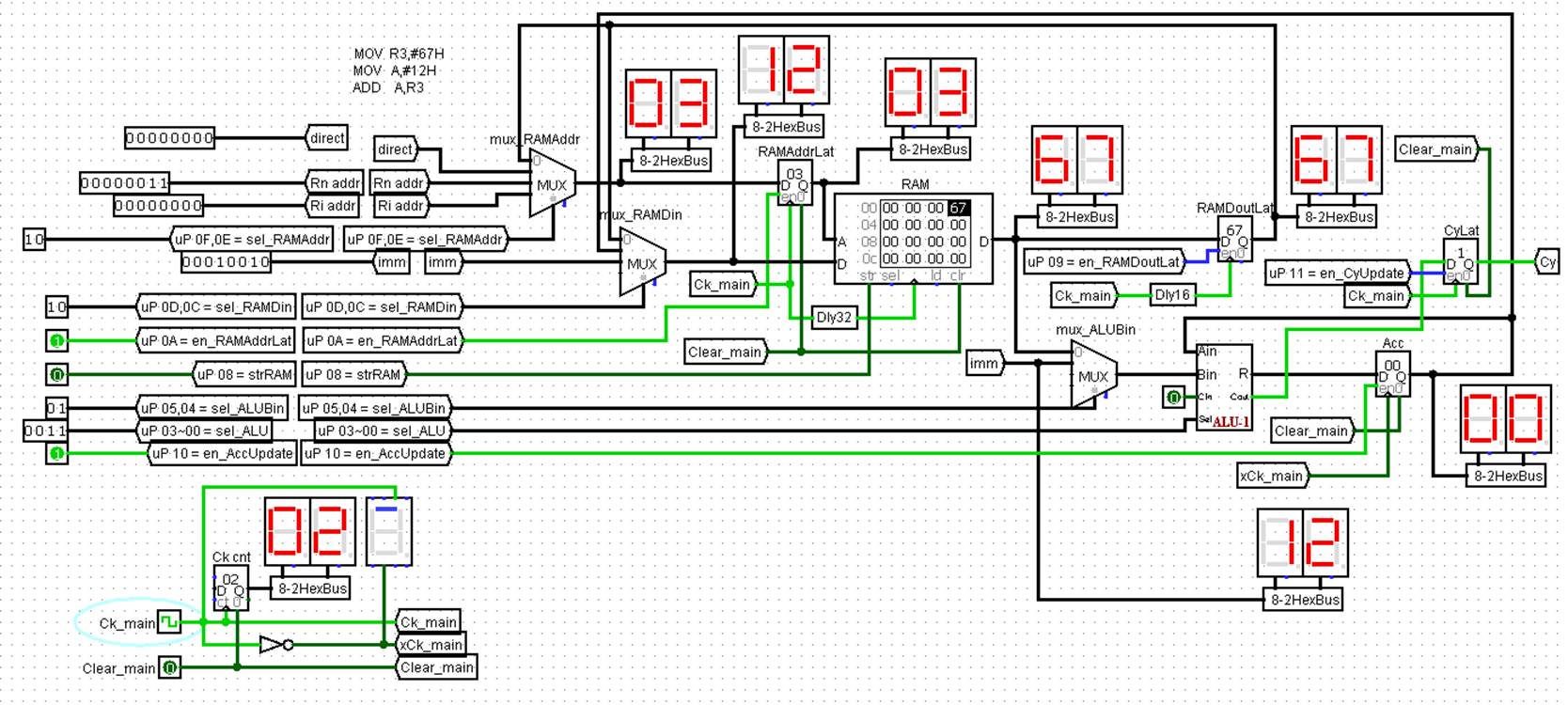
After negative edge of CK
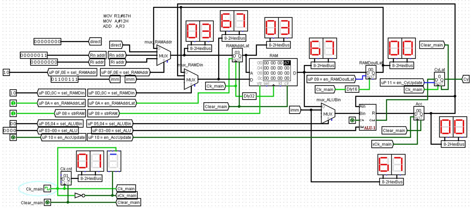
![]()
Before
running MOV A,#12H
![]()
After positive edge of CK
![]()
After negative edge of CK (Note: Acc has been updated.)
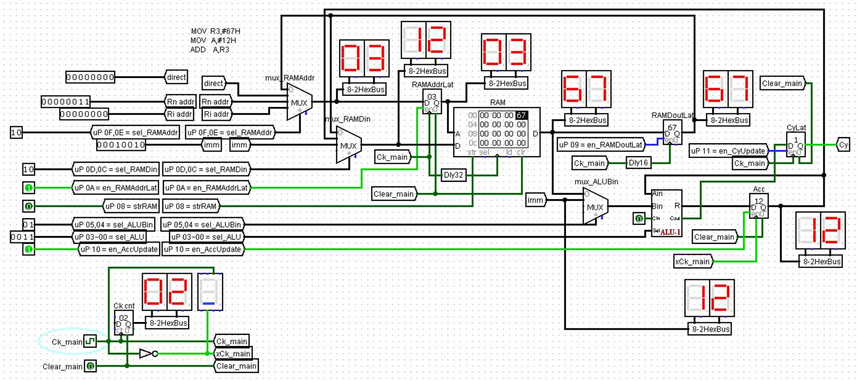
![]()
Before
running ADD A,
R3

After positive edge of CK
![]()
After negative edge of CK
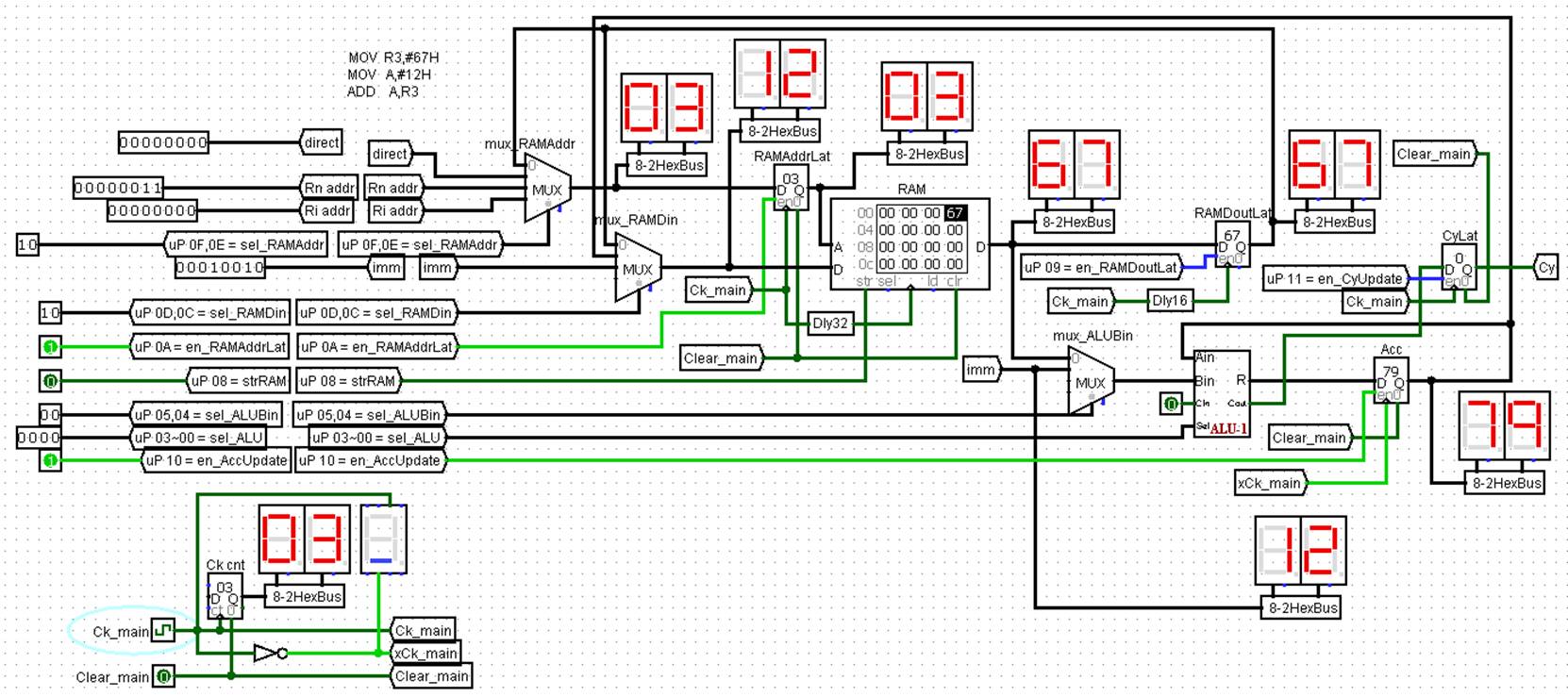
![]()