|
Practice 1: Build an application circuit for RAM with
the data interface of “synchronous load/store port”. |
|
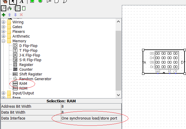
Step 1: Select the “Memory” type “RAM”. Choose the “Data Interface” of “One synchronous load/store port”. Choose “Address Bit Width” and “Data Bit Width”. |
|
|
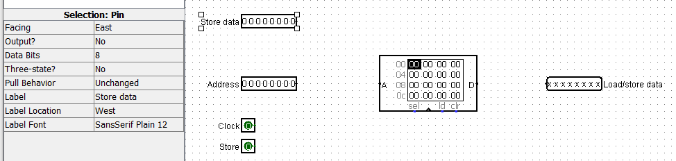
Step 2: Add the input pins and output pins. “Output?” is to specify whether it is an input pin or an output pin. Choose a number in “Data Bits” for the desired bit number. Give each pin a label. Choose the pin direction in “Facing”. |
|
|
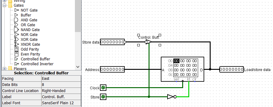
Step 3: Connect the components with wire. Add Controlled Buffer and NOT Gate where needed. |
|
|
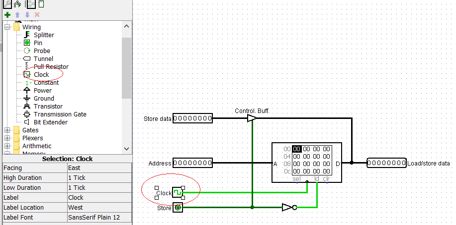
Step 4: Replace the Clock input pin with a clock source. |
|
|
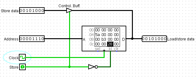
Step 5: Store data into the memory. |
|
|
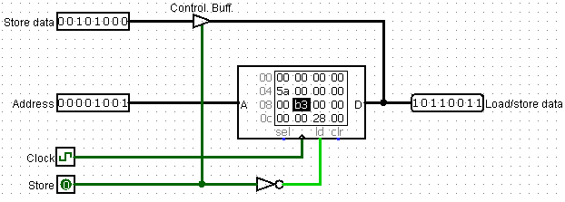
Step 6: Read data to the output pins. |
|
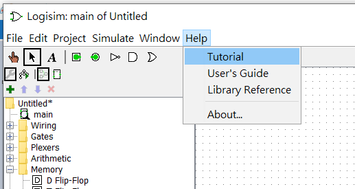
Consult “Help”/“Tutorial” or “User’s Guide” for detailed usage guide.