|
Note: Most of the content in this page is
duplicated from Logisim document! Source of this
page: |
RAM
|
Library: |
|
|
Introduced: |
2.0 Beta 1 |
|
Appearance: |
|
Behavior
The RAM component, easily the most
complex component in Logisim's built-in libraries, stores up to 224 = 16,777,216 values (specified in the
Address Bit Width attribute), each of which can include up to to 32 bits (specified in the Data Bit Width attribute).
The circuit can load and store values in RAM. Also, the user can modify
individual values interactively via the Poke Tool, or the user can modify the
entire contents via the Menu Tool.
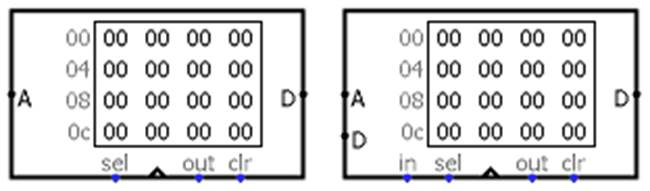
Current values are displayed in the
component. Addresses displayed are listed in gray to the left of the display
area. Inside, each value is listed using hexadecimal.
The value at the currently selected address will be displayed in inverse text
(white on black).
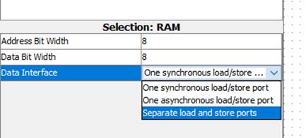
The RAM component supports three different interfaces, depending on the Data
Interface attribute.
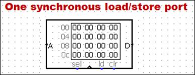
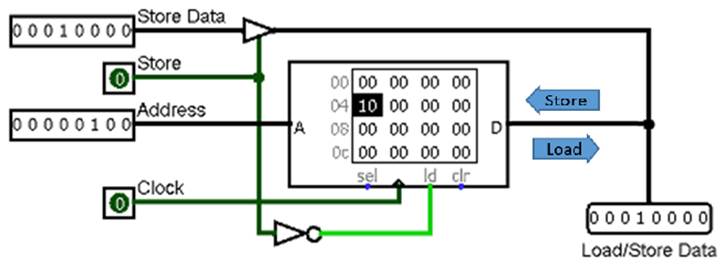
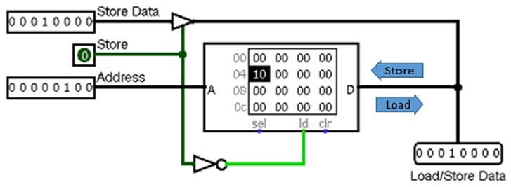
One synchronous load/store port (default)
The
component includes a single port on its east side that serves for both loading
and storing data. Which it performs depends on the input labeled ld: 1
(or floating) indicates to load the data at the address designated on the
component's west side, and 0 indicates to store the data given on the port. To
transmit data into and out of the component, you will need to use a Controlled
Buffer component, as illustrated below.
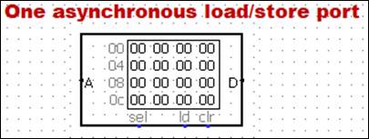
One asynchronous load/store port
This
is the same as above, except that there is no clock.
The value found on the data bus is stored into memory whenever the ld
input is 0. If, while the ld input is 0, the address or data changes,
then an additional store occurs. This option is meant to more closely
approximate the interface of many available random-access memories.
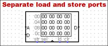
Separate load and store ports
Two
data ports are provided - one on the west side for storing data, and another on
the east side for loading data. This option removes the necessity of dealing
with the Controlled Buffer and so it is easier to use.
Pins
A
on west edge (input, bit width matches Address Bit Width attribute)
Selects which of the values in memory is currently being
accessed by the circuit.
D
on west edge (input, bit width matches Data Bit Width attribute)
This input is present only if "separate load and store
ports" is selected for the Data Interface attribute. When a store is
requested (via the clock changing from 0 to 1 while sel and str
are both 1 or floating), the value found at this port is stored into memory at
the currently selected address.
D
on east edge (input/output or output, bit width matches Data Bit Width
attribute)
If sel and ld are 1 or floating, then the RAM
component emits the value found at the currently selected address on this port.
If there is a single load/store port, the value read from this port is stored
whenever a store is requested.
str on south edge (input, bit width 1)
Store: This input is present only if "separate load and
store ports" is selected for the Data Interface attribute. When it is 1 or
floating, a clock pulse will result in storing the data found on the west edge
into memory (provided the sel input is also 1 or floating).
sel on south edge (input, bit width 1)
Chip select: This input enables or disables the entire RAM
module, based on whether the value is 1/floating or 0. The input is meant
primarily for situations where you have multiple RAM units, only one of which
would be enabled at any time.
triangle on south edge (input, bit
width 1)
Clock input: This is absent when the Data Interface
attribute's value is "One asynchronous load/store port." In other
circumstances, when ld is 0, and this input rises from 0 to 1 (and sel
is 1/undefined and clr is 0), then the value at the currently selected
address changes to whatever value is at the D pin. As long as the clock
input remains 0 or 1, though, the D value will not be stored into
memory.
ld
on south edge (input, bit width 1)
Load: Selects whether the RAM should emit (on D) the
value at the current address (A). This output behavior is enabled if out
is 1 or undefined; if out is 0, then no value is pushed onto D -
but if there is a combined load/store port, stores will be enabled.
clr on south edge (input, bit width 1)
Clear: When this is 1, all values in
memory are pinned to 0, no matter what the other inputs are.
Attributes
When the component is selected or being
added, the digits '0' through '9' alter its Address Bit Width attribute and
Alt-0 through Alt-9 alter its Data Bit Width attribute.
Address Bit Width
The bit width of the address bits. The number of values
stored in RAM is 2addrBitWidth.
Data Bit Width
The bit width of each individual value in memory.
Data Interface
Configures which of the three interfaces are used for
communicating data into and out of the component.
Poke
Tool Behavior
See poking memory in the User's Guide.
Text
Tool Behavior
None.
Menu
Tool Behavior
See pop-up menus and files in the User's
Guide.