Notes on Programming and Debugging 8051 with Edsim51


Topic

$


Rn or ARn?     A or Acc?

#HIGH(…), #Low(…)


nybble


using

Addressable bits in RAM (e.g. 2FH.7)

ORG


$

Description

$ represents the address of the current instruction.

Example


0000| ADD A,R0

0001| ADD A,R0

0002| JMP $

0004| ADD A,R0

0005| ADD A,R0


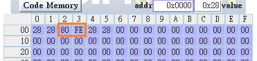
Note: (For signed numbers)

02H – 04H = FEH  


#HIGH(…) , #Low(…)

Description

#HIGH(…) represents the high byte of the address

#LOW(…) represents the low byte of the address

Example


MOV DPH,#HIGH(table_of_number_to_7_segment_code)   

MOV DPL,#LOW(table_of_number_to_7_segment_code)   


table_of_number_to_7_segment_code:

db 11000000B ; 0 = C0H

db 11111001B ; 1 = F9H

db 10100100B ; 2 = A4H

db 10110000B ; 3 = B0H

db 10011001B ; 4 = 99H

db 10010010B ; 5 = 92H

db 10000010B ; 6 = 82H

db 11111000B ; 7 = F8H

db 10000000B ; 8 = 80H

db 10010000B ; 9 = 90H

db 10001000B ; A = 88H

db 10000011B ; B = 83H

db 11000110B ; C = C6H

db 10100001B ; D = A1H

db 10000110B ; E = 86H

db 10001110B ; F = 8EH


Exercise

After you run the instructions in the example above, what will be the content of DPH and DPL?


Addressable bits in RAM (e.g. 2FH.7)

Description

The following examples show you how to program with the addressable bits.

Examples

SETB       2FH.0

SETB        78H      ; The same as    SETB 2FH.0

CLR         21H.7

CLR         0FH       ; The same as    CLR   21H.7


Nybble

Definition

A nybble = a half of a byte

Example

0110 1110 1100 contains 3 nybbles.


ORG

Attribute

An assembler directive

Format

ORG   addr

Description

ORG is an assembler directive. It specifies a location in the code memory for the instruction below this directive. In other words, it directs the assembler to put the machine code of the subsequent instruction in the specified address.
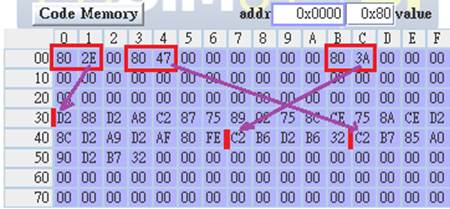
 

Example 1

Example 6 on the edsim51 website:

ORG 0                          ; reset vector
        JMP main               ; jump to the main program

ORG 3                          ; external 0 interrupt vector
        JMP ext0ISR            ; jump to the external 0 ISR

ORG 0BH                        ; timer 0 interrupt vector
        JMP timer0ISR          ; jump to timer 0 ISR


ORG 30H                        ; main program starts here

main:
        SETB IT0               ; set external 0 interrupt as edge-activated
        SETB EX0               ; enable external 0 interrupt
        CLR P0.7               ; enable DAC WR line
        MOV TMOD, #2           ; set timer 0 as 8-bit auto-reload interval timer

        MOV TH0, #-50          ; | put -50 into timer 0 high-byte - this reload value,
                               ; | with system clock of 12 MHz, will result in a timer 0 overflow every 50 us

        MOV TL0, #-50          ; | put the same value in the low byte to ensure the timer starts counting from
                               ; | 236 (256 - 50) rather than 0

        SETB TR0               ; start timer 0
        SETB ET0               ; enable timer 0 interrupt
        SETB EA                ; set the global interrupt enable bit
        JMP $                  ; jump back to the same line (ie: do nothing)

; end of main program


; timer 0 ISR - simply starts an ADC conversion
timer0ISR:
        CLR P3.6               ; clear ADC WR line
        SETB P3.6              ; then set it - this results in the required positive edge to start a conversion
        RETI                   ; return from interrupt


; external 0 ISR - responds to the ADC conversion complete interrupt
ext0ISR:
        CLR P3.7               ; clear the ADC RD line - this enables the data lines
        MOV P1, P2             ; take the data from the ADC on P2 and send it to the DAC data lines on P1
        SETB P3.7              ; disable the ADC data lines by setting RD
        RETI                   ; return from interrupt


      ORG 0                           ; reset vector

0000|   JMP main               ; jump to the main program


      ORG 3                           ; external 0 interrupt vector

0003|   JMP ext0ISR            ; jump to the external 0 ISR


      ORG 0BH                         ; timer 0 interrupt vector

000B|   JMP timer0ISR          ; jump to timer 0 ISR


      ORG 30H                         ; main program starts here

      main:

0030|   SETB IT0               ; set external 0 interrupt as edge-activated

0032|   SETB EX0               ; enable external 0 interrupt

0034|   CLR P0.7               ; enable DAC WR line

0036|   MOV TMOD, #2           ; set timer 0 as 8-bit auto-reload interval timer


0039|   MOV TH0, #-50          ; | put -50 into timer 0 high-byte - this reload value,

                                      ; | with system clock of 12 MHz, will result in a timer 0 overflow every 50 us


003C|   MOV TL0, #-50          ; | put the same value in the low byte to ensure the timer starts counting from

                                      ; | 236 (256 - 50) rather than 0


003F|   SETB TR0               ; start timer 0

0041|   SETB ET0               ; enable timer 0 interrupt

0043|   SETB EA                ; set the global interrupt enable bit

0045|   JMP $                  ; jump back to the same line (ie: do nothing)


      ; end of main program


      ; timer 0 ISR - simply starts an ADC conversion

      timer0ISR:

0047|   CLR P3.6               ; clear ADC WR line

0049|   SETB P3.6              ; then set it - this results in the required positive edge to start a conversion

004B|   RETI                   ; return from interrupt


      ; external 0 ISR - responds to the ADC conversion complete interrupt

      ext0ISR:

004C|   CLR P3.7               ; clear the ADC RD line - this enables the data lines

004E|   MOV P1, P2             ; take the data from the ADC on P2 and send it to the DAC data lines on P1

0051|   SETB P3.7              ; disable the ADC data lines by setting RD

0053|   RETI                   ; return from interrupt


The machine code for Example 6 of the edsim51 website:


Note: (For signed numbers)

          02H + 2EH = 30H,     05H + 47H = 4CH,       0DH + 3AH = 47H
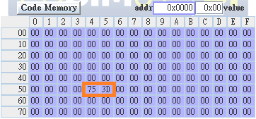
 

Example 2

Using “ORG” to specify the locations for storing data in the code memory:

ORG  54H

DB     75H

DB     3DH


The corresponding machine code:


Rn or ARn?       A or Acc?

In edsim51, “ARn” and “Acc” are treated as offset.

They can be used in instructions that contains an “offset” field.

                                                                                         Some examples are shown in the table below.         

Example

O/X

(Correct / wrong)

Instruction Format

CJNE  A,R3,AGAIN

X

CJNE   A,direct,offset

CJNE  A,AR3,AGAIN

O

PUSH   R6

POP   R6

PUSH   A

POP   A

X

PUSH   direct

POP   direct

PUSH   AR6

POP   AR6

PUSH   Acc

POP   Acc

O

ADD   A,A

X

ADD   A,direct

ADD   A,Rn

ADD   A,Acc

ADD   A,AR5

ADD   A,R5

O

INC   AR4

INC   R4

O

INC   direct

INC   Rn


Below are some more explanations.       

Syntax

Acceptable by edsim51:

PUSH   ARn

POP      ARn                       (n = 0, 1, 2, …, 7)

Unacceptable by edsim51:

PUSh    Rn

POP      Rn

Explanation

The machine code of PUSH:

11000000

direct

The machine code of POP:

11010000

direct


PUSh/POP can only use the direct addressing mode for their operand. Hence, it must be an 8-bit direct address of RAM, instead of a 3-bit encoding for registers.

In edsim51, “ARn” stands for an 8-bit address, hence it is acceptable. On the other hand, “Rn” appearing in an assembly instruction implies the 3-bit encoding of registers, hence “PUSH/POP Rn” is not acceptable.

Example

average:

    PUSH PSW
    PUSH AR0
    PUSH AR1
    MOV  B, R1
    CLR  A

loop:

    ADD  A, @R0

    INC  R0

    DJNZ R1, loop
    DIV  AB
    POP  AR1
    POP  AR0

    POP  PSW
    RET

Similar cases


Instruction


ADD


Instruction

Syntax

Machine code


ADD  A,A      

X


ADD A,Acc   

O


Q: Why is “ADD A,A” syntactically wrong?

A: The first operand “A” is implicitly specified by the opcode. The second operand “A” is not allowed because 8051 doesn’t provide such a double implicitity.

Note: The “ADD” instruction allows the following four addressing modes:

ADD A,#imm

ADD A,@Ri

ADD A,direct

ADD A,register


ADD A,A is not allowed.


DEC


Instruction

Syntax

Machine code

DEC R7

O

0001 1111

DEC AR7

O

0001 0101 0000 0111

Q: Why are both DEC R7”and “DEC  AR7”syntactically correct?

A: That is because DEC has both register addressing and direct addressing modes.


Note: The “DEC” instruction allows the following four addressing modes:

DEC @Ri

DEC A

DEC direct

DEC register


Summary


Using

Attribute

An assembler directive

Format

Using 0

Using 1

Using 2

Using 3

Description

One of the four register banks is used for the registers R0 ~ R7.

“USING “ is an assembler directive that indicates to the assembler which register bank is being used.

Example 1

using      0                              ; The register bank 0 will be used.

  MOV      R0, #30H              ; initialize the subroutine by putting the start address into R0

  MOV      R1, #05H              ; and by putting the size of the set into R1

  CALL      fillInNumbers

  CALL      average_B

  JMP                       $


The End


To add

MOV  B,#9H

MOV A,#-5

ADD A,B

MOV A,#0FBH

ADD A,B              

MOV A,#-05H

ADD A,B

assembler directive: 

Topic: How to specify a bit in the program?

JB  P1.3, AAA

JB  93H,AAA

JB  90H.3,AAA


;   JB  PSW.4,AAA    ; Wrong

JB  0D0H.4,AAA