Explanation on Example
6
|
Example 6 Function |
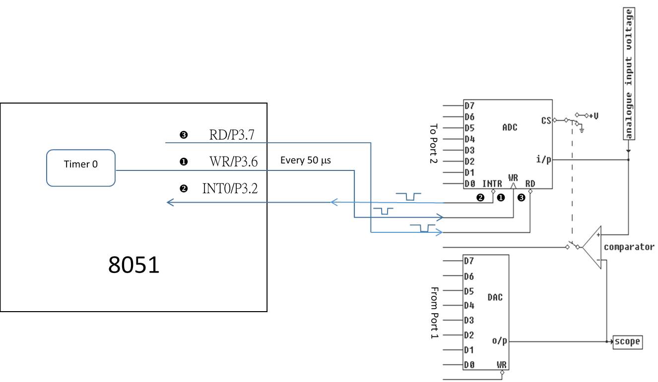
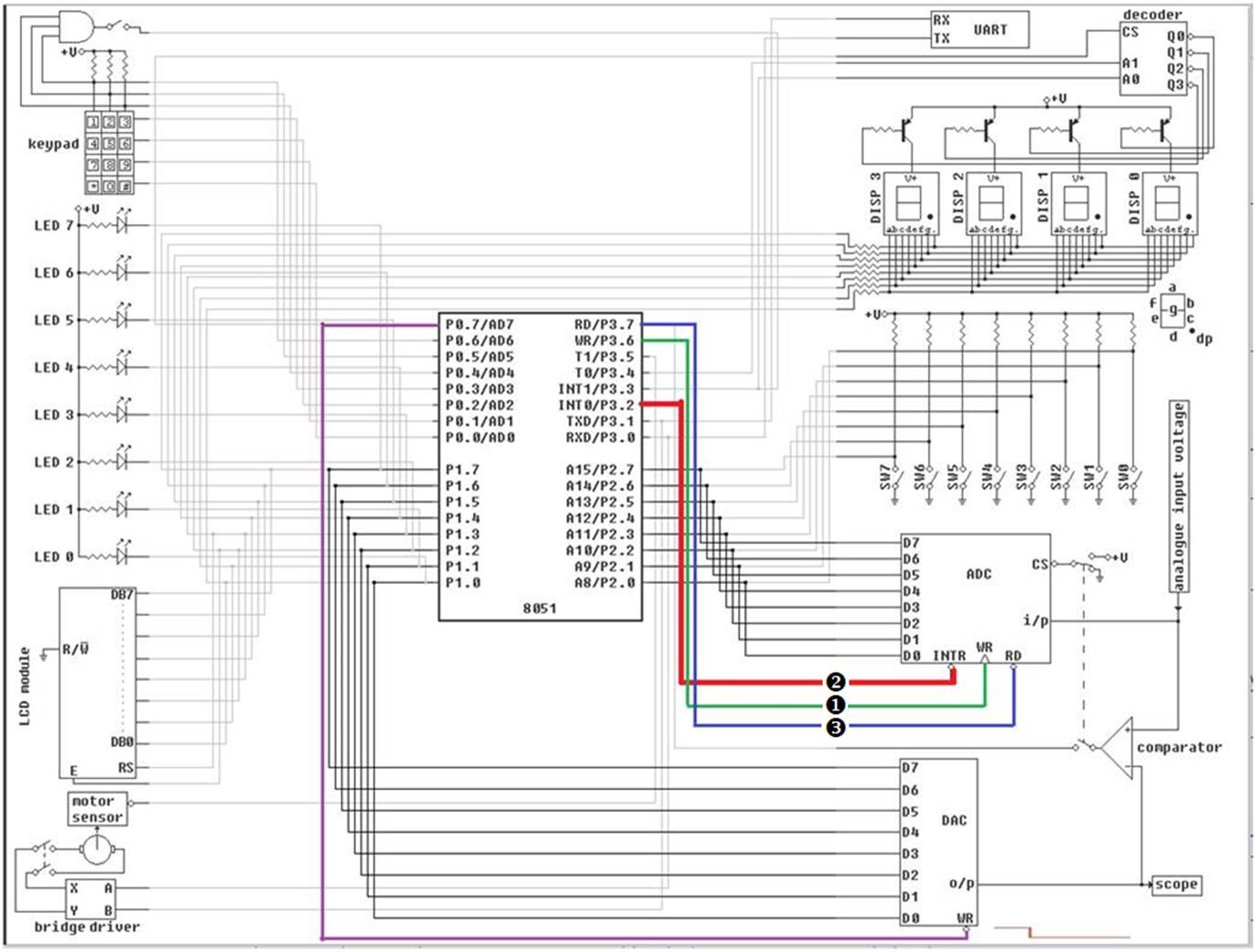
This Example 6 program reads the analogue
input voltage at the ADC input and displays it on the scope via the DAC. |
|
Step u |
The processor triggers the ADC to conduct an A-to-D conversion every 50 us. To trigger, the processor creates a positive edge on the signal WR. To maintain the 50 us period, the processor utilizes Timer 0 to constitute a 50-us timer. |
|
Step v |
When the ADC completes an A-to-D conversion, it creates a negative edge on the signal INTR. This signal serves as an external interrupt to the processor. |
|
Step w |
After the processor receives the external interrupt from the ADC, it puts the RD pin of the ADC at the low level. The low level on the RD signal enables the output D7~D0 of the ADC. The processor reads the ADC output at Port 2 and then moves it to Port 1, for the input of the DAC. |
|
|
Note: The ADC can convert an analog voltage into a binary number in 25 us. |

Actions in Example 6:
|
This program reads the analogue input voltage
on the ADC and displays it on the scope via the DAC. This is achieved by setting timer 0 to
interrupt the main program every 50 us. This line is interfaced with the 8051 external
0 interrupt line. The external 0 ISR therefore takes the reading
from the ADC on P2 and passes it to the DAC on P1. (ie: until the next timer 0 interrupt). ADC enabled; comparator disabled. Comparator enabled; ADC disabled. |
ADC
Pin Function
|
Name |
Direction |
Value |
Function |
|
WR |
Input |
Positive edge |
Initialize an Analog-to-Digital conversion |
|
Otherwise |
No effect. |
||
|
INTR |
Output |
Positive edge |
Issue an interrupt to inform the processor that a conversion has been finished. |
|
Otherwise |
No effect. |
||
|
PD |
Input |
PD = 0 |
Enable the output D7~D0 The data pins become lo-Z. The data can be read by the processor |
|
PD = 1 |
Disable the output D7~D0. The data pins become hi-Z. The data cannot be read by the processor. |